
Compound Semiconductor Hub – Scaling up Manufacturing with Atoms
Future Compound Semiconductor Manufacturing Hub
Advanced Compound Semiconductor materials underpin many societal priorities such as net zero and the ‘Connected Nation’, and UK manufacturing is contributing to the next generation of mass-market products with new production techniques.
Professor Peter Smowton Head of Cardiff University’s School of Physics and Astronomy and Future CS Hub Director

Above: Optical image of 150mm wafer – each small square on the image contains 100 VCSELs
Compound Semiconductor (CS) materials are a key enabling technology underpinning the operation of data centres, the internet backbone connectivity and smartphones, the internet of things (IoT), satellite communications/GPS, energy efficient lighting and displays, electric vehicles, efficient solar power generation and advanced healthcare.
The demands of next-generation technologies are driving the integration with – or replacement of – silicon with advanced CS materials, creating a truly massive market opportunity for CS materials and devices.
The manufacturing of compound semiconductors is more involved than that of silicon with the need to put together atoms and different layers of atoms, each often only a few atomic layers thick to benefit from quantum effects, and to do this uniformly over increasingly large areas – currently more than 150 and 200mm diameters.
This atomic layer epitaxy and the crystals it produces then have to be structured in three dimensions using fabrication techniques akin to those used in the silicon industry but compatible with a much wider variety of materials.
While the companies and brands that utilise this key enabling technology are often international, the UK is a leader in the manufacturing of the materials and increasingly further along the manufacturing supply chain.
CS Hub Exemplar Output: Manufacturing the VCSEL
Vertical Cavity Surface Emitting Lasers have several mass-market applications including as the light source for the facial recognition system in the latest smartphones.
VCSELs are created from as many as 200 individual crystal layers that either guide light (in which case they are of the order of 200 billionths of a metre thick – 200 10-9 m) or guide electrons (in which case they are of the order of 5 billionths of a metre thick 5 10-9 m; a human hair is about 1000 times thicker).
The individual crystals often have a slightly different lattice constant meaning the atoms making up the different layers would like to be at a different separation in each layer. This causes stress and as one tries to make these structures at larger scale, the wafer (crystal) will bow.
Instead of working on a flat surface, the machining of the semiconductor has to be done on a surface where the height changes by 10,000 or more times the layer thickness and more than any feature size required.
Together with epitaxy manufacturer, IQE, the CS Hub is working on approaches to facilitate this manufacturing. This involves innovation in the crystal growth, in the fabrication or 3D structuring and in developing automated on wafer testing of the individual devices.


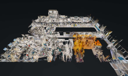
Above and below: Electron microscope images, side view (showing crystal layers and etched mesa) and top view of metal contacts to individual VCSEL. 153,600 VCSELs are fabricated on a 150mm diameter wafer with a less than 2% variation in mesa height across the wafer
